

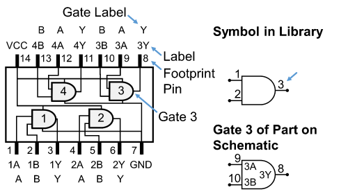
Parts include logical information, and associations with schematic symbols and PCB footprints. A gate can either be a traditional logic element with a device, such as an AND gate, or a section of the device I/O, such as an FPGA (Field Programmable Gate Array) I/O bank. Power signals can also be included within gates. The division of selected sets of part pins into gates is defined by a Pin Assignment. A simple example is illustrated below of a Quad 2-Input AND Part and schematic symbol.
In this case, each symbol represents a simple logic gate. The values in the following table are shown in the Symbols section, in the Part Editor panel, Detail tab. This information is shown when you select a part in eCADSTAR Library Editor, and then select Edit > Part on the assist menu.
| Symbol Information in Part Detail | Definition | Value in this Example |
|---|---|---|
| Gate Count | Specifies the number of gates for the part. | 4. |
| Gate | The gate number. | 1, 2, 3 or 4. |
| Name | Specifies the Symbol that is used for a particular gate. | For example, “AND_GATE”. |
| Alternate | Can be used to specify an alternate symbol for the gate. | No alternate, so left blank. |
| Pin Count | The number of pins on the symbol for this gate. | 3. |
The Pin Assignment section in the Part Editor Panel, Detail tab contains the mapping between physical part pins and gates. It is described in the following table.
| Pin Assignment Information in Part Detail | Definition | Values in this Example |
|---|---|---|
| Pin Count | The total number of pins on the part. | 14 |
| Footprint Pin | The physical pin name or number on the part. | Values range from “1” to “14” |
| Label | The pin label, which must be unique for the part. For example, if there are two GND pins, then they cannot both be labelled “GND”. | Unique labels “1A”, “1B”, “1Y”, “GND”, “VCC”, etc. These are shown in the image above. |
| Circuit Label | The circuit label, which does not have to be unique. For example, you can have more than one circuit label with the value “GND”. | In this example, these are blank. However, If you populated Circuit Label, you would still use the names described for Label because, for example, “1Y”, “2Y”, etc. do not necessarily connect to the same signal on the schematic. |
| Type | The pin type in terms of I/O or another function. | POWER, GROUND, INPUT, OUTPUT. |
| Gate | The gate number that includes the physical pin. | 1, 2, 3 or 4. |
| Symbol Pin | The unique number that identifies the pin on the symbol. When you select a row in the Pin Assignment section, you can choose from available Symbol Pin numbers. These represent the pin positions on the symbols. They are not the same as physical pin numbers. | In this case, the symbols are gates with two input pins and one output pin, as shown in the above image. This symbol is used to represent each of the four gates in the part. In all cases, the Symbol Pin value is either 1, 2 or 3. |
| Gate Label | This value must be unique within the gate. Gate Label is the name of the signal on the pin, at the gate level. | In this case, the Gate Label value, as shown in the above image is either “A”, “B” or “Y”. Compare this value to Label and Circuit Label, which represent the pin signal at the part level. |
| Signal | The name of a power or ground signal as it exists on the schematics. This field is used for implied power, where the power and ground pins are not shown on the symbol. | In this case, the gate symbol applies only to logic pins, and not to “VCC” and “GND”. Consequently, pin 7 in the image above would be set to Signal “GND”, and pin 14 would be set to Signal “VCC”. This method of assignment is less common for devices with large numbers of power and ground signals, such as FPGAs (Field Programmable Gate Arrays). In which case, I/O bank power signals, for example, are usually included in symbols. |
