The template areas that you create on the canvas in eCADSTAR PCB Editor are listed in the Template Area List dialog. For a template area that you select in the dialog, its properties are displayed in the Properties panel. You can change its priority, pen width and the template parameters in the Properties panel. The template area is also displayed on the canvas when you select it in the Template Area List dialog. Launch this dialog by clicking Net /Route > Template Area > Template Area List on the eCADSTAR PCB Editor ribbon.
Template areas are created on the canvas using the Area Fill (Polygon), Area Fill (Rectangle) or Area Fill (Circle) command. Select ON in the Template area field.
| Value | Description |
|---|---|
| ID | The numeric identifier that is automatically assigned to the template area when you create it. When you select a row in the Template Area List dialog, this value is displayed in the Template Area ID field in the Properties panel. |
| Layer | Displays the conductor layer on which the relevant template area is created. |
| Net | Shows the net that is associated with the template area when it was created. |
| Priority | For overlapping area fills, this defines the order in which
they are flooded with copper. A lower value represents a higher
priority. Area fills with a higher priority are processed before
those with a lower priority. The overlapping area is assigned
the net associated with the area fill of the highest priority.
Values between 1 and 100 are displayed.
|
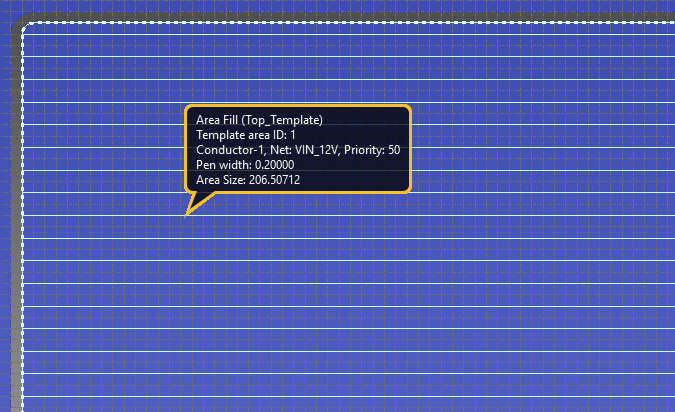
| Pen width |
Shows the distance between the copper tracks that are added to the template area. You can change this value by selecting a row in the Template Area List dialog, and then specifying a value in the Properties panel, Pen Width field. Tracks are added in the X direction. If you specify a value of "0.2",with a grid pitch of "0.1", then the tracks in the template area are created as shown below.
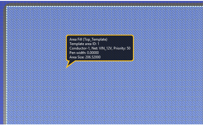
If you specify a value of "0", then the template area is filled with solid copper. This is shown below.
|
 button.