
PCB Design: Technology Library Import
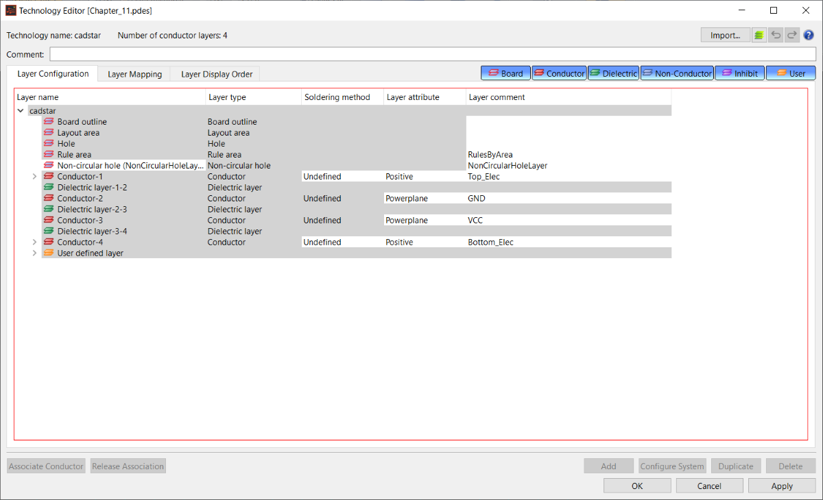
During the migration process, a localized technology (layer stack up) is created for the design, and is associated with the localized library data. After the initial migration, this technology is not aligned with the eCADSTAR Master Library. A process to import the relevant technology from the library will update the mapping between Master library elements and the design content.
- Launch eCADSTAR PCB Editor.
- Select File > Open to launch the Open dialog.
- Browse to the location of the migrated design, and select the [design].pdes file.
- Click Open to load the design into eCADSTAR PCB Editor.
- On the Home tab, Design Rules group, select Technology Editor to open the design’s Technology Editor dialog.
- Click the Import button to open the Import (Technology Library) dialog.
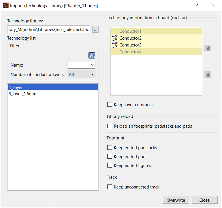
- Select the required technology from the Technology Library list.
- Ensure that all check boxes are deselected, and then click Overwrite to import the data from the technology library to the design.
- To continue, click Yes in the confirmation dialog.
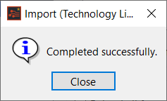
- Confirm any messages in the Import (Technology Library) report dialog.
- Click Close to close the report and continue.
- Click Close in the confirmation dialog.
- Click Close in the Import (Technology Library) dialog.
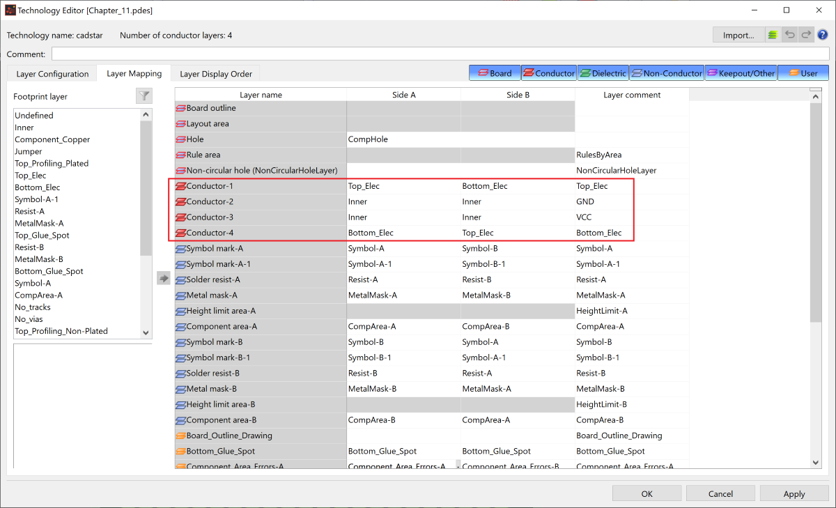
- In the Technology Editor dialog, select the Layer Mapping tab. The updated conductor layer mapping is shown, which has been imported.
- Click OK in the Technology Editor dialog to apply the imported changes.
- Click File > Save to save the changes to the design.
Note
If there were any instance-based changes in the CADSTAR design, then the Keep edited padstacks, Keep edited pads and Keep edited figures check boxes should be selected.
If there were any instance-based changes in the CADSTAR design, then the Keep edited padstacks, Keep edited pads and Keep edited figures check boxes should be selected.
