
Performing Back Annotation to the Schematic Design
To align the schematic to the associated PCB design, the Back Annotation process should be performed.
- Launch CADSTAR Design Editor.
- Select File > Open. The Open dialog is displayed.
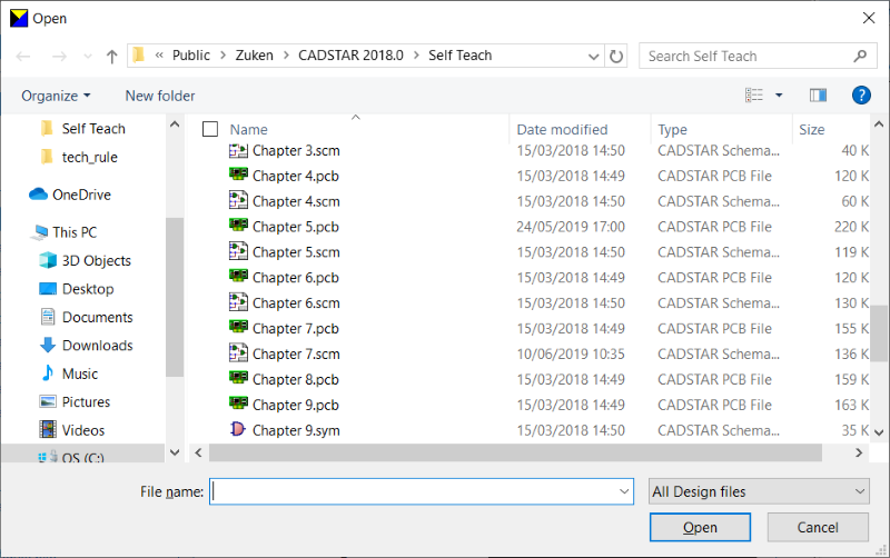
- Use the dialog to browse to the location of the schematic, and click Open to open the design in the CADSTAR Design Editor.
- Confirm and close any dialogs that are displayed.
- On the ribbon, select Back Annotation in the Design tab, Back Annotate group. The Back Annotation dialog is displayed.
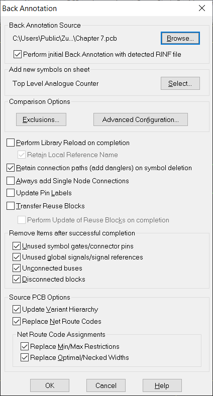
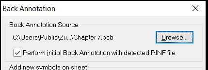
- Click the Browse button to open the Back Annotation Source File dialog. Use the dialog to browse to the location of the design, and click Open to select it.
- Review the options in the dialog for the updates to be performed, and click OK to proceed. If Component renames are required, then the Back Annotation Summary dialog is displayed. Otherwise, the Collating Schematic Design dialog is displayed.
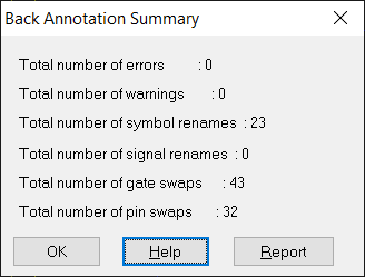
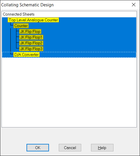
- Ensure that all sheets are selected and click OK. The ECO Update process is performed. When completed, a Back Annotation report is displayed.
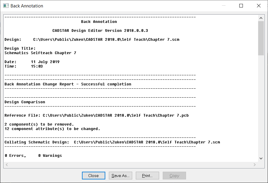
- Click Close in the Back Annotation report dialog. If changes are made, then you are prompted to accept them. Confirm the changes to be applied to the design.
Note
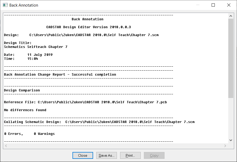
- It is recommended to perform a second Back Annotation Update operation to confirm that designs are fully aligned. This is indicated by the "No differences found" notification in the Back Annotation report dialog.
- Any errors displayed in the ECO Update report dialog must be resolved in CADSTAR to ensure that the PCB and schematic can be aligned.
- Click File > Save to save the changes to the design.
