
The voltage driven common mode algorithm calculates the radiation due to a noise voltage. This could be between a heatsink or a signal trace, and any cables attached to the board when it is not located in a shielded enclosure. The common-mode current on cables driven by a voltage-driven source is induced by the electric fields that couple to cables from a trace or other structures. Another voltage driven EMI mechanism is I/O Coupling.
I/O Coupling
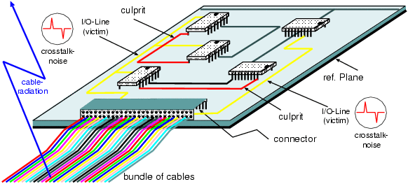
The Radiation by I/O Coupling algorithm calculates the radiated field that is caused by common mode noise coupled to the I/O nets. The noise voltage coupled to the I/O nets (victim) from other nets (culprits) on the same board may drive the cables attached to the I/O net. This may result in significant radiation. The following image illustrates this coupling mechanism.
In the PI/EMI analysis module, the I/O Coupling algorithm works in the following three steps.
- Noise Voltage calculation
- Antenna Current Calculation
- Emission Estimation
These steps are explained in more detail in the following sections.
Noise Voltage Calculation
In order to compute the coupled noise voltage between aggressor nets and I/O-nets for each frequency, the coupling parameters C’m and L’m for the capacitive and inductive coupling must be derived from the geometry of the tracks. Important parameters for this calculation are the coupled length and the coupling distance. These values are derived for each individual segment of the I/O-net.
In order to perform a worst case analysis, potential tracks between an aggressor and a victim net are ignored.
Based on the coupled segments, the coupled noise voltage VNoise(f) is calculated. Both inductive and capacitive coupling are calculated. The larger value of VCap(f) and VInd(f) is applied as the driving voltage source for the I/O-segment currently being considered. For each I/O-segment, the maximum noise voltage of all aggressor segments is stored and added to the total I/O-net coupled noise voltage VNoise(f) for all frequencies f. In parallel, the voltage contributions are stored and added for each aggressor net individually. This enables the aggressor’s contributions to be listed later.
The following Figure provides an example for two aggressor nets acting on a single I/O-net, at a given single frequency.
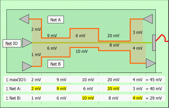
The maximum noise voltage VNoise for the individual net segments may be caused by different aggressor nets, as indicated in yellow in the above image. This may lead to the result that the total I/O noise voltage is larger than any of the aggressor’s contributions. This is shown in the example with 45 mV total I/O noise voltage, but 40 mV or 29 mV as the individual contributions.
The reported voltage values are in the frequency domain rather than the time domain, which is usually used to calculate crosstalk.
In the PI/EMI analysis module, the local distribution of the coupling voltage can be visualized on the canvas in eCADSTAR PCB Editor .
Antenna Current Calculation
The algorithm calculates the radiation from each I/O net, which is extended onto an attached cable. The attached cables are assumed to be in resonance for all frequencies. See: Assumptions.
The number of power/ground pins in the connector (and therefore in the cable as well) determine how much of the crosstalk signal is a common mode current or a differential mode current. In the extreme case that no power/ground pin is present, the majority of the current is assumed to not return easily. Hence, the emission will be very high. Additionally, the filtering of individual pins is also accounted for in the algorithm. This information can be viewed and edited in the Classification dialog.
In the PI/EMI analysis module, the emission per I/O net is reported in the PI/EMI Analysis module: Radiation dialog. The five worst contributing electrical signal nets can be viewed, with their related emission, by selecting them on the assist menu. This allows you to quickly identify the critical coupling paths on the board.
Common mode emission is a far field phenomenon. Therefore, a minimum Antenna Distance of 3m is required in the PI/EMI analysis module.
