
The Output (ODB++) dialog
allows you to export ODB++ data from a design. The parameters in the dialog
can be imported from a file, and saved from the dialog to a file. The
Output (ODB++) dialog is displayed by clicking
Manufacture > Manufacture Output >  ODB++
on the ribbon. ODB++ versions 7.0 and 8.1 are supported.
ODB++
on the ribbon. ODB++ versions 7.0 and 8.1 are supported.
| Item | Description | |
|---|---|---|
| Import parameters | Allows you to import settings to this dialog by selecting a parameter file in the Open dialog and clicking Open. | |
| Export parameters | Allows you to save the settings specified in this dialog. Add a location and file name in the Save As dialog, and click Save. | |
| ODB++ destination folder | Shows the location of the folder into which the ODB++ file is exported. | |
 |
Displays the Select Folder dialog. Set the location of the folder into which the ODB++ file is exported, and click Select Folder. | |
| ODB++ job name | Specify the job name that is associated with the ODB++ data. By default, the name of the PCB design is displayed. | |
| ODB++ format version | Specify the ODB++ format that the data is exported to. | |
| 7.0 | Data is exported to ODB++ version 7.0. | |
| 8.1 | Data is exported to ODB++ version 8.1. | |
| Execute | Exports the ODB++ data using the specified parameters. | |
| Exit | Closes this dialog without exporting ODB++ data. |
Specify Layer Tab
The Specify Layer tab allows you to set the parameters for each layer in the design.
Custom settings
| Item | Description | |
|---|---|---|
| Merge same attribute layers (Symbol mark, Solder resist and Metal mask) | When multiple symbol mark layers, solder resist layers or metal mask layers exist for a particular conductor layer, then you can specify whether they are merged and output to a single ODB layer. | |
| Selected | If multiple symbol mark layers, solder resist layers or metal mask layers exist for a particular conductor layer, then they are merged and output to a single ODB layer. | |
| Not selected | If multiple symbol mark layers, solder resist layers or metal mask layers exist for a particular conductor layer, then they are output to multiple ODB layers. | |
| View filter | Allows you to filter the layer information that is shown in the Layer table. | |
| Output | If selected, then the layers for which the Output target check box is selected are shown in the Layer table. | |
| Not output | If selected, then the layers for which the Output target check box is not selected are shown in the Layer table. | |
| Layer table | Specify the layers that are exported from the design, and the ODB++ layer name that is associated with each exported layer. | |
| Layer name | Shows the layers in the design. | |
| Output target | If selected, the layer in the Layer name column is exported to the layer in the ODB ++ layer name column. | |
| ODB++ layer name | Specify the ODB++ layer name for each exported layer. If left blank, then the default layer name is used. |
| Item | Description | |
|---|---|---|
| Expand non-component plated padstacks to include adjacent layer pairs | If required, you can specify whether drill data for plated
holes in padstacks is also output for each individual layer, rather
than just outputting drill data for the defined layer spans.
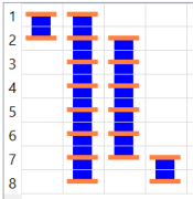
Note If Use core layer is selected in the Rule Editor Dialog: Board Tab, then the padstacks in core layers are not expanded. This setting is illustrated using the following example of the layer spans for an 8-layer board with no core layers.
The following layer spans are defined.
If Expand non-component plated padstacks to include adjacent layer pairs is not selected, then drill data for just these layer spans is output. If selected, then drill data for plated holes is output for each individual layer. The following additional layer spans would therefore be output.
Note The specified setting is saved, regardless of whether eCADSTAR PCB Editor is closed. |
|
| Selected | Drill data for plated holes is output for each individual layer,
as well as drill data for the defined layer spans. For example,
if the layer spans 1-2, 1-8, 2-7 and 7-8 are defined for a board,
then drill data is output for the following layer spans.
|
|
| Not selected | Drill data is output only for the defined layer spans. These are listed in the Hole From-To column. Drill data for plated holes is not output for individual layers. | |
| Drill Layer table | Allows you to set the ODB++ layer name to which drill data for holes is exported. | |
| Hole From-To | Shows the layer span value for the relevant hole. | |
| Output target | If selected, then drill data is exported for the relevant layer span. | |
| ODB++ layer name | Set the layer name to which drill data is exported. If left blank, the default layer name is used. |
Others Tab
The Others tab allows you to specify the logical information and user attributes that are exported from the design.
| Item | Description | |
|---|---|---|
| Comment | Allows you to associate a comment with the exported ODB++ data. | |
| Logical Information | Set whether to export information that is assigned in conductor layers for components and nets, and whether to export netlists. | |
| Output components and net information assigned to data in conductor layers | If selected, information is exported that is assigned in conductor layers for components and nets. | |
| Output netlist | If selected, netlists are exported. | |
| Attributes | Allows you to specify whether to export user-defined attributes that are assigned to parts of components as attribute information. User-defined attributes are specified in the Attribute Manager dialog. | |
| Output attributes | If selected, then the Available attributes box is made available. Specify the user attributes that are exported. | |
| Available attributes | If Output attributes is selected,
then specify the user attributes that are exported by selecting
an attribute and clicking  . .
|
|
|
|
Select an attribute in the Available
attributes box, and then click to move
it to the Attributes to Output box.
Multiple attributes can be selected using the Ctrl
or Shift key. |
|

|
Select an attribute in the Attributes
to Output box, and then click to move
it to the Available attributes box.
Multiple attributes can be selected using the Ctrl
or Shift key. |
|
| Attributes to Output | Shows the user attributes that are exported. Add or remove
items using the and
buttons, respectively. |
