In eCADSTAR, a library is a master folder where symbols, parts, footprints, technologies (layer-stack definitions) and design rules are stored and edited. This centralization allows the creation and editing of library data to be more easily controlled. When you create a schematic or PCB design, eCADSTAR Schematic Editor and eCADSTAR PCB Editor reference the single library. The path to the library is specified in the Product Settings dialog in eCADSTAR.
Library Structure
The library structure is shown below. There are further levels of detail that are not shown, such as pads and padstacks.
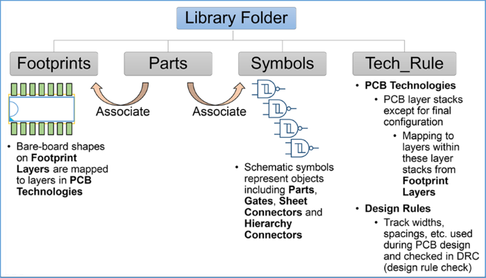
Each part has an associated footprint which defines its bare-board shape. You can also associate a footprint with a 3D model that represents the package shape. Parts can be associated with schematic symbols. Symbols can also represent objects, including the following:
- Non-physical items such as connections to power supply voltages or off-sheet connectors.
- Gates or other subsets of the I/O pins of a part.
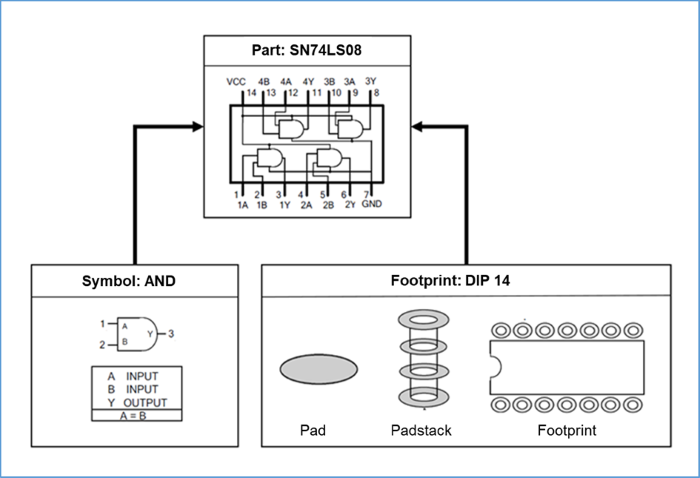
The relationship is illustrated below between the part, symbol and footprint in a traditional QUAD 2-Input AND (SN74LS08), with DIP14 package.
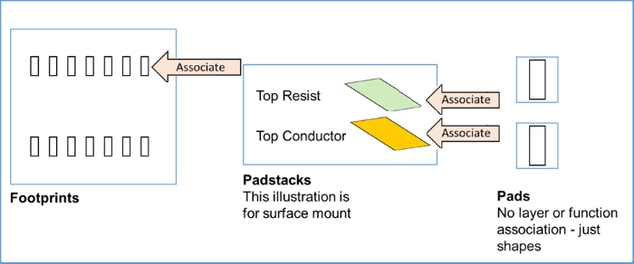
The relationship between footprints, padstacks and pads is shown below. Footprints include figures such as assembly shapes, and define the layout of the padstacks or pads within them. As padstacks contain definitions on multiple footprint layers, such as Top Elec, Inner and Solder Resist, it is most common to place them within footprints.
Padstack definitions include references to footprint layers, whereas pad definitions include no layer associations. It is useful to define items such as pads so that they can be re-used. However, if you place them in the footprint as padstacks, then their footprint layers may conflict with each other. In this case, solder resist, conductor and solder paste pads can be placed directly on the correct layers within the footprint.