
Multiple technologies can be defined within the same library. Technologies reside in the Technology and Rules branch of the library, as shown below.
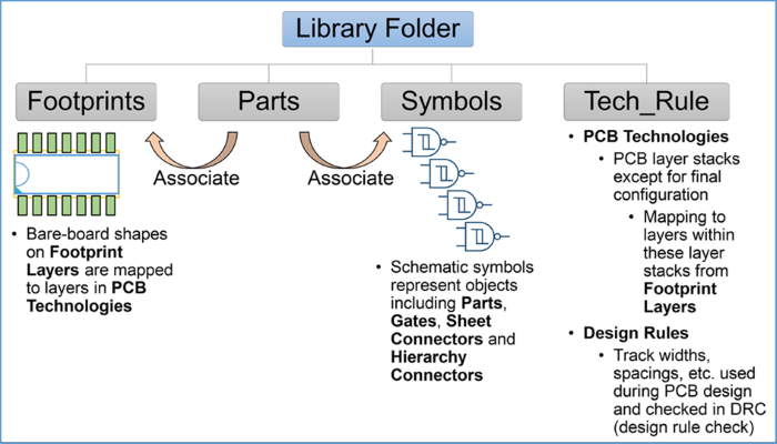
Each technology contains the following items.
- A PCB layer stack called “Layer Configuration”. This does not contain the final details that are added when the PCB is created.
- A technology, and therefore also the layer stack within it, is referenced by each PCB design.
- The mapping from footprint layers to layers within the layer stack that is defined in the technology.
Mapping from Footprint Layers to Technology Layers
The image and table below show the following.
- The most basic set of footprint layers that you might use in designing surface-mount footprints.
- A layer configuration within a technology that could reference these footprint layers.
- The mapping from footprint layers to PCB layers. This is defined within the technology.
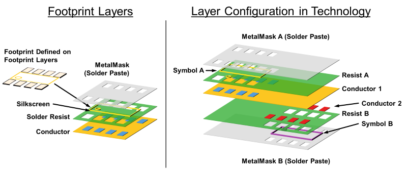
The following table shows the mapping from the basic footprint layers to the PCB Technology Layers, for a surface mount example.
| PCB Layer in Technology | Mapped Footprint Layer (PCB Side A) | Mapped Footprint Layer (PCB Side B) |
|---|---|---|
| MetalMask A, MetalMask B | MetalMask | MetalMask |
| Symbol A, Symbol B | Silkscreen | Silkscreen |
| Resist A, Resist B | Solder Resist | Solder Resist |
| Conductor 1, Conductor 2 | Conductor | Conductor |
Footprint layers can be referenced by one or more PCB layers in the layer configuration defined in the technology. The mapping on sides A and B can either be the same or different. In this example, MetalMask, Silkscreen and Solder Resist layers are mapped to corresponding technology layers on Side A and Side B. If a footprint requires different treatment on Side A and Side B, then separate footprint layers are needed. For example, the soldering process might require different pad sizing, depending on whether a component is mounted on Side A or Side B.
The 8-layer stack shown below is suitable for through-hole components. Resist and conductor shapes differ on Side A and Side B, but the six inner layers are all mapped to the single Conductor Inner footprint layer.
Side A and Side B on the PCB do not necessarily correspond to top and bottom layers. They are viewpoints. If the top conductor layer is Conductor 1 and the bottom conductor layer is Conductor 7, and these layers are in sequential order in the Layer Configuration, then:
- The Side A mapping shown in the table below
applies to the layer stack viewed from the top side.
- The Side B mapping applies to the layer stack viewed from the bottom side.x
This is why, for example, Footprint layer Solder Resist A is mapped to Resist A for Side A and to Resist B for Side B.
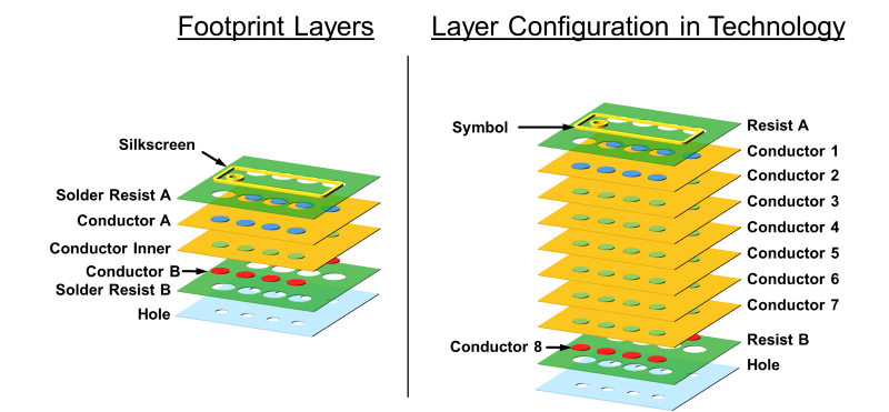
The following table shows the mapping from basic footprint layers to PCB technology layers, for a through-hole example.
| PCB Layer in Technology | Mapped Footprint Layer (Side A) | Mapped Footprint Layer (Side B) |
|---|---|---|
| Symbol | Silkscreen | Silkscreen |
| Resist A | Solder Resist A | Solder Resist B |
| Conductor 1 | Conductor A | Conductor B |
| Conductor 2 to Conductor 7 | Conductor Inner | Conductor Inner |
| Conductor 8 | Conductor B | Conductor A |
| Resist B | Solder Resist B | Solder Resist A |
| Hole | Hole | Hole |
