
Power Integrity Analysis
The Power Integrity (PI) analysis within the PI/EMI analysis module of a power bus is divided into the following steps. These are performed automatically.
- Identification of individual power supply systems
- Estimation of the transient switching current of the ICs
- Calculation of the overall
power bus impedance.
This includes the following. - Power planes
- Decoupling capacitors (decaps)
- Computation of the Power
Bus Noise Voltage, in time- and in frequency domain
The following are derived from this. - Power bus emissions
- Receiver noise margin checks
Apart from the RF behavior of the supply system, the DC behavior can be inspected as well.
Identification of Supply Systems
In an initial step, the PI/EMI analysis module distinguishes the supply nets into groups of "Power" and "Ground" type nets. This is based on net attributes. If these are missing, then net names can be interpreted instead in order to determine the net type. Names such as "GND" and "VCC", "3.3V" etc. are recognized. See: Supply: Power or Ground. However, any specific setting made in the design system is preferred.
To set up a complete supply network, you may need to connect individual supply nets across passive elements. The Connect dialog in the Classification dialog, Supply tab allows you do this. See: Setting up the Supply System. All combinations of "Power" and "Ground" supply system pairs where ICs or decaps are connected will now be identified. Those combinations with no further components attached to the pair are not considered valid power busses. All others are listed in the Power Bus dialog. For this selection mechanism, it is helpful if the power or ground pin types are properly set on the IC.
Transient Switching Current
Every time a logic device switches, a short but strong current peak occurs during the transition. This so-called crowbar current or shoot-through current flows from the VCC to the GND port of the inverter during the time when both transistors are conducting.
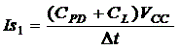
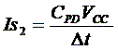
This switching current iS(t) can be approximated by a triangular-shaped current peak that has peak values Is1 and Is2. This is shown below.
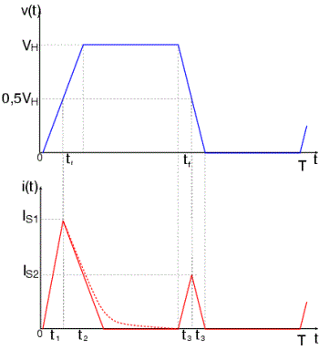
The timing parameters t1, t2, and t3 are derived from the trapezoidal output signal of the buffer. Note that t2 is load dependent, as
 .
.
Cpd is the power dissipation capacitance of the IC. This value is stored in the simulation library. CL is the load capacitance.
Based on this switching current iS(t), a Fast Fourier Transform (FFT) is performed to obtain the switching current IS(f) in the frequency domain.
Power Bus Impedance
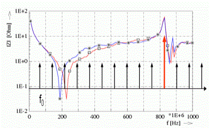
Power Plane Pairs are typically used to provide the switching current to the ICs in a higher frequency range where decoupling capacitors can no longer work efficiently ( f>20-50 MHz ). A constant, low impedance of the power plane pair is therefore required in a wide frequency range between the fundamental clock frequency f0 of the ICs, up to 10, 15, or 20 harmonics of the clock frequency f0 shall be considered.
From DC up to a low number of MHz, Power Plane Pairs exhibit capacitive behavior. The power plane impedance is calculated as Z=1/jwC. This frequency range is basically determined by the size and shape of the power plane pair.
At higher frequencies, power plane pairs can act like cavity resonators, as known by microwave designers. When the field within the plane is excited by some high-frequency current, electromagnetic waves travel from this excitation point towards the boundaries of the plane pair.
The plane's boundaries provide a strong impedance mismatch, hence the waves get reflected.
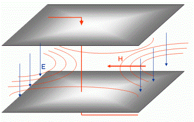
Some of these waves may cancel each other, and others will cause additive interferences. Hence, standing waves are likely to occur at certain frequencies, where the dimensions of the planes are equal to half of the wavelength, or multiples of this. These distinct field patterns are called cavity modes.
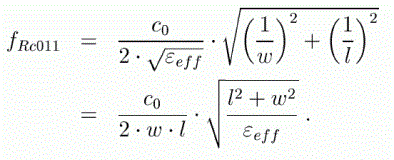
For rectangular cavities, the resonant frequencies fRc can also be determined analytically.
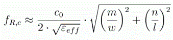
With m = 0; 1; 2;... ; n = 0; 1; 2;... ; where m and n are the order of the cavity mode. The values w, and l are the X, Y dimensions of the plane. The above equation is a good approximation of the cavity mode equation in 3D, when the height of the cavity is very small compared to the length and width of the plane. For the first two-dimensional mode, the equation simplifies to the following.
Since the current distribution within the planes is strongly related to the electromagnetic field between them, local extrema in the current distribution are created at these modes. In areas of low current densities, a connected IC cannot easily get current from the plane pair. This transfers to a higher impedance in these areas. The impedance of a pair of power planes is therefore no longer following the pure capacitive behavior of lower frequencies, but shows an oscillating behavior once the first resonant frequency is reached.
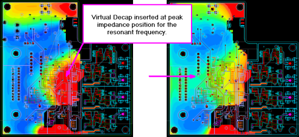
The following images show the local distribution of the plane impedance Z(x,y,f) at resonant frequencies.
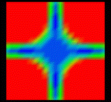
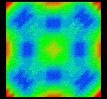
If one or more harmonics of the IC's clock frequency coincide with a plane’s resonant frequency, then the IC’s function may fail if the supply pins of the IC are within a high-impedance area. This is the red area in the above images.
As indicated above, one of the clock's harmonics may hit a peak in the power bus impedance. This will cause a high noise voltage in the supply system, a large emission and may lead to failure of the IC. This depends on the required amount of current at that frequency.
Impedance Calculation
Within the PI/EMI analysis module, the input impedance Z(f) is computed at all supply pins of the active components (ICs). This includes all connecting network elements such as tracks, vias, power plane pairs and passive components (for example, decoupling capacitors (decaps)).
This network impedance analysis Z(f) is done in the following two-step approach.
- Individually characterize all network elements for their input and transfer impedances. This involves a numerical computation of the power/ground plane pair impedances.
- Combine all elements into the complete Power Net's network, and compute the input impedance at the IC's power pins.
For this purpose, the power and ground pins of the ICs must be properly defined in the Simulation Library. Check the power pin settings in the Classification dialog, Pin Tab. Both the pin type and signal type are listed here. If necessary, correct the pin type within the Digital IC Editor of the Simulation Library Manager.
The input impedance of the power/ground plane pair is calculated differently, depending on the size of the power plane pairs.
- For small plane pairs with a longest edge length
less than 20 mm, or less than 9 grid points, a simple plate capacitor
formula is applied. This is because small planes do not show any resonance
within the frequency range of 1 GHz. Such a small copper shape is
modeled as a PI-element.
- For all other plane pairs, a numerical approach
is applied. The precise shape of the overlapping areas of the power
and ground plane is discretized into small squares with a given grid
size. For each of the grid cells, an equivalent R, L, C network is
applied. This is similar to the PI element shown above, for each edge
in the grid. Each cell contains a capacitance at the corners of the
grid, a resistor and an inductor at the edges of the cell. The capacitive
and inductive behavior of the power plane pair is modeled in this
way. The resistive losses of the conductors are included. All combined
grid elements form a potentially huge electrical network.
The grid size can be specified in the Options dialog. It should at least be smaller than l/10, where l is the shortest wavelength to be considered (l=c/f)). However, in most practical cases, the given geometry of the power planes requires a much finer grid size. This is typically in the range 0.1mm to a few mm.
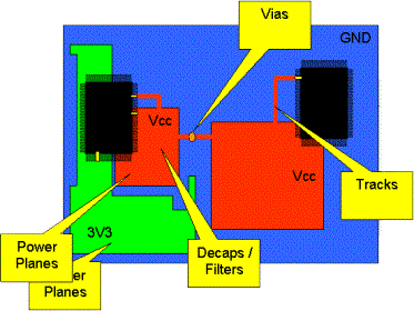
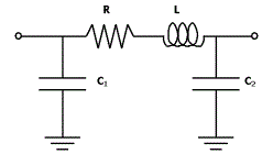
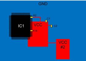
Within this R, L, C network of the overlapping area, decaps and ICs are contained with their respective equivalent circuit, as shown below. The component's power pin is inside the overlapping area. Further elements, such as through tracks connecting other plane pairs, for example, are not considered. This allows you to see the individual impact of a particular plane pair. In the image below, the decap C1 and IC1 pin A14 are included within the impedance distribution. Decap C2 and IC1 pin A2, which are connected through tracks are not considered. The impact of the second power plane pair connected by a track are not considered in the impedance distribution of the first plane pair. In any situation, all components are included within the overall PI network, to compute the input impedance over frequency.
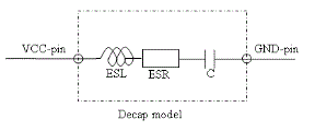
The decap impedance consists of the capacitor with ESL and ESR values that are defined in the Options dialog, and the inductance of vias used to connect them to the power planes. Most importantly, the impedance of the tracks connecting the decap and the vias is also included. These values are listed for all capacitors in the Power Bus dialog, Decap tab.
The Virtual Decaps functionality allows you to explore the impact of adding more decoupling capacitors (decaps) before actually placing a new component in the design.
Noise Voltage and Emissions
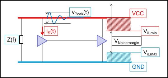
The current iS(t) which is drawn by a switching gate, such as an output buffer within an IC, causes a voltage drop within the supply system. This is mainly due to the inductive behavior of the supply system. When this noise voltage within the supply system becomes too large, the correct operation of the circuits may be affected. Hence, the noise voltage is reported in both the time and frequency domain. The noise voltage level can be read as a measure for the quality of the overall supply system.
- In the time domain, the peak-to-peak noise voltage is determined. This can consequently be compared with the noise margin of the input buffers. A large vPeak value may fully consume the noise margin of the input buffers so that the input buffers cannot properly determine whether the logic level is low or high. In calculating the peak voltage, it is assumed that the output buffer will switch under all circumstances, and therefore acts as a noise current source. This may result in fairly high noise voltage values, which are above the supply voltage level shown in the result column of the Power Bus Common view. In these cases, the supply system has quite a high impedance. This may be due to missing or too small power planes and decoupling capacitor (decaps).
- In the frequency domain, multiplying the switching
current IS(f) with the impedance Z(f) yields a noise voltage spectrum
V(f)Noise. The image below shows the mechanism and the related voltages.
This noise voltage upon the supply system may drive the power planes, acting as an antenna. The radiated electric field strength in the far field is calculated as follows.
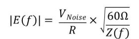
R is the Antenna Distance. The antenna impedance of an isotropic radiator is 60 Ω.
This power bus emission is a far field phenomenon. Therefore, a minimum Antenna Distance of 3m is required in the PI/EMI Analysis Module.
