
As well as the High-Frequency behavior of the Supply System, its DC-behavior is of interest to PCB designers. As many electronic consumer products are small and light-weight, the relevant PCB structures must be as small as possible. Supply Systems are often designed with very little safety margin, hence the so called IR-drop within traces and copper shapes may cause failures of the active devices. Also, thermal problems may occur because of over-loaded vias, or narrow traces and copper structures.
The main purpose of the DC-Analysis functionality is to check if the supply voltage levels at the active component’s power pins are acceptable, or if a voltage drop occurs somewhere in the supply system which is too high. The results of the DC-Analysis are presented in the DC IC table, in the Power Bus dialog. If the supply voltage levels become critically low, then the tool indicates the reasons for the voltage drop in the supply system which is too high. These will be related to high-resistive elements in the supply system. For example, a too narrow trace, a single via in the main current path, or a narrow path within a copper shape.
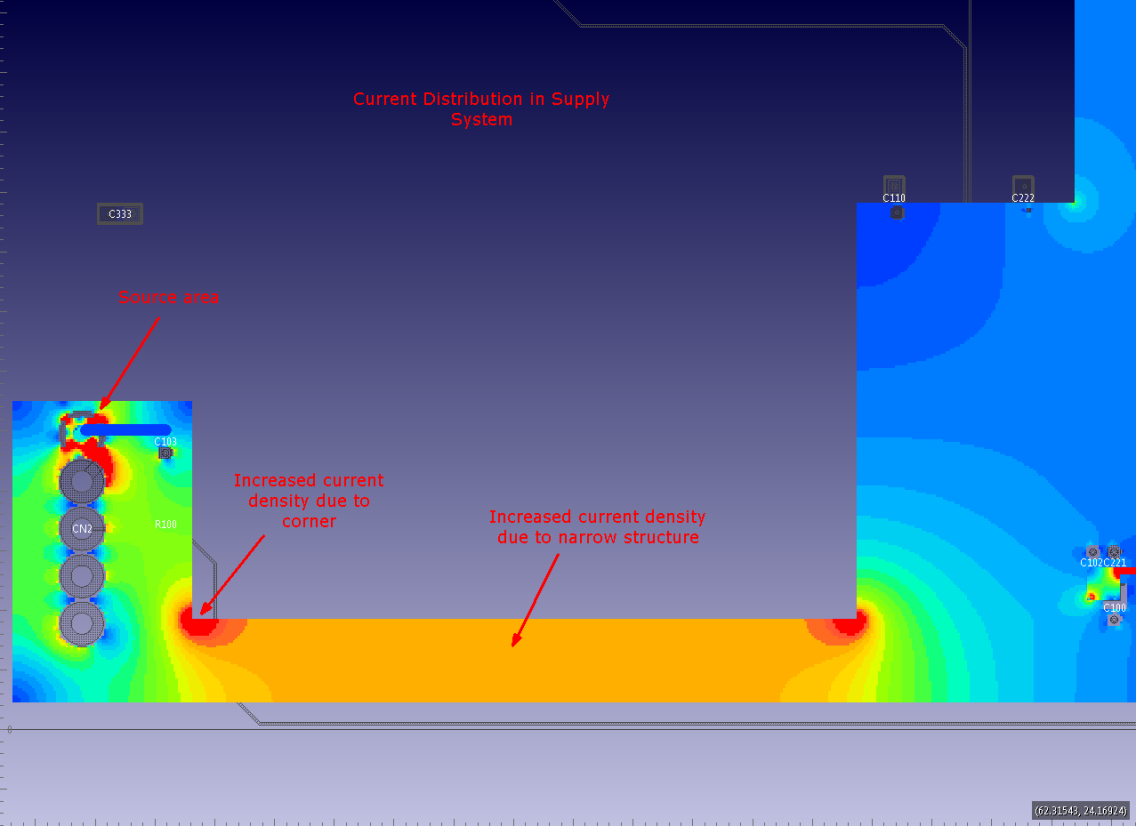
The DC resistance values between the DC Analysis source pins and the supply pins of the ICs are listed on the Power Bus level, as well as individually for each IC. Also, the voltage drop across individual vias is shown in the DC Via table in the Power Bus dialog. For the track and copper shapes, the results are shown as a 2D current and voltage distribution.
The image above shows the magnitude of the current distribution computed for a network composed of tracks, planes and vias. The DC Analysis book in the Online Help shows how DC Analysis is done within the PI/EMI Analysis Module.
- The DC Analysis uses settings in the Classification dialog, and in the Options dialog, DC tab.
- Details on the algorithmic background are provided here.
