
Task 8: Routing Branched Address Signals
In this topic, you will route the signals to topologies using the DIY_HS_1_Partial_Routed.pdes design. This design contains all the required Skew Groups.
- Open the partially routed design, DIY_HS_1_partially_routed.pdes. In this task, you will route one of the address signals.
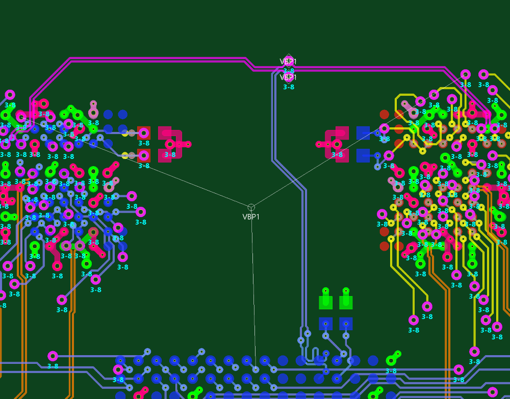
Figure 1: Unrouted Address Signal
- On the eCADSTAR PCB Editor ribbon, select View > Canvas > Routing Balloon. The Routing Balloon is displayed on the canvas.
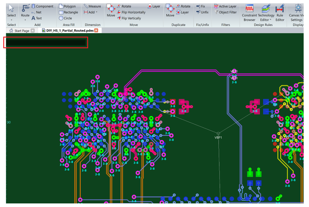
Figure 2: The Routing Balloon
- Click the routed Differential Pair. Some of the dependencies that are required to route it are displayed in the Routing Balloon. A red bar is displayed at the bottom of the Routing Balloon. This shows the maximum pin pair length of 45 mm that is set for the Differential Pair.
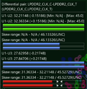
Figure 3: The Routing Balloon
- On the Status Bar, ensure that Conductor-3 is set as the active layer.
- On the canvas, deselect the differential pair that you selected.
- On the ribbon, select Net/Route > Routing > Add Route. The Add Route dialog is displayed.
- Start to route the unconnected net associated with the LPDDR2_CA[0] signal. Continue routing it until you reach the top point between the SDRAMS, shown below.
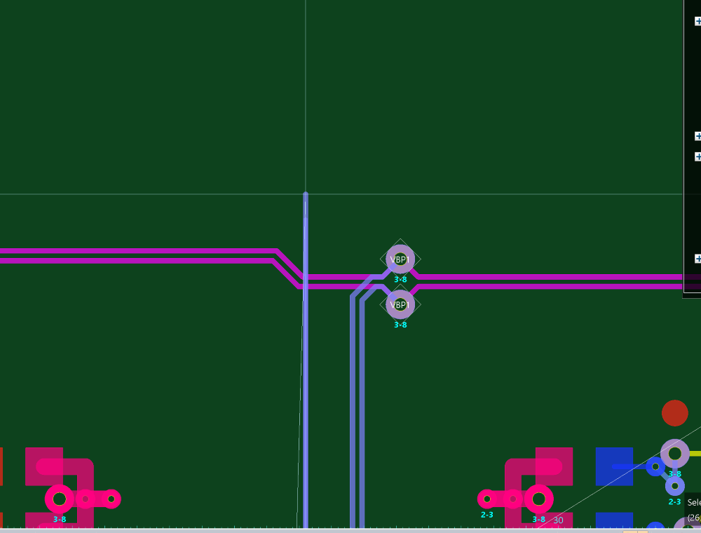
Figure 4: Routing an Unconnected Net
- Double-click the mouse to place a via. In the displayed Active Layer dialog, select "Conductor-7" or press "7" on the keyboard to set it as the active layer. A via is placed on the canvas.
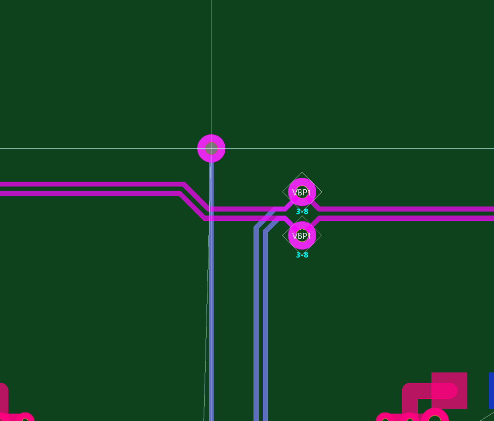
Figure 5: Placing a Via
- Right-click, and select Collect Next Virtual Branch Point on the assist menu. The virtual branch point will snap to the via.
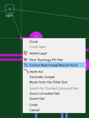
Figure 6: Collect Next Virtual Branch Point
You can then route either way from it.
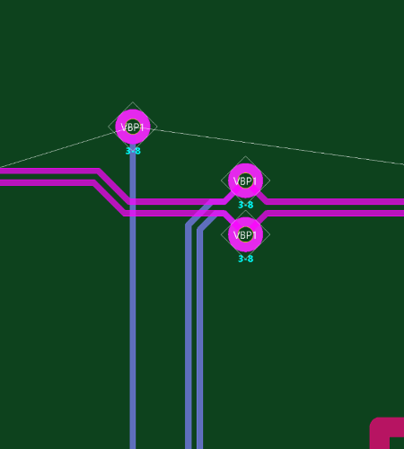
Figure 7: Routing from a Virtual Branch Point
Note
If you make an adjustment to the routing of a partially-routed net, then the virtual branch point may be disconnected from the via. The virtual branch point is then placed in a centralized position between the unrouted nets.
- Click the via to continue routing. The track is routed to the unconnected net marker on the right.
- Right-click, and select Next Topology Pin Pair on the assist menu. The pin pair that is currently being routed is switched, to route towards the memory module.
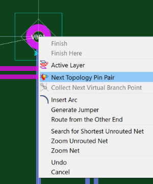
Figure 8: Routing to the Next Topology Pin Pair
- To finish routing the pin pair, continue routing to the first memory module.
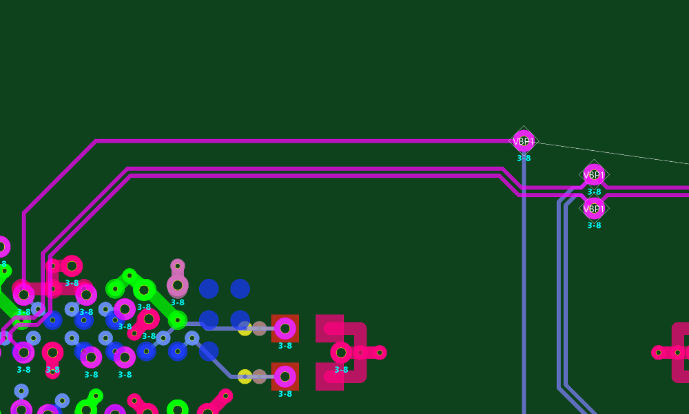
Figure 9: Routing to the First Memory Module.
- Finish routing the other pin pair to complete the routing of the LPDDR2_CA[0] signal.
- Save the design as MyHSDesign2.pdes. This completes the routing task for the High Speed training. Next you will lengthen the design to constraints.
Next topic: Task 9: Applying Batch Lengthening
