The Fan-out command allows you to generate fan-outs for a component, or for component pins that you select on the canvas.
- When you select a component, the command attempts to generate fan-outs for all the pins on the component.
- When you select a component pin, the command attempts to generate fan-outs for the selected pin.
This command is launched by clicking Padstack > Pad/Padstack > Fan-out on the eCADSTAR PCB Editor ribbon (only available in 2D View mode).
Note
The "To" layer that you specify in the From-To field must be set to "visible", or fan-outs will not be generated. This is done by selecting the (Visible
layer) column for this layer in the Layer
Settings Panel.
(Visible
layer) column for this layer in the Layer
Settings Panel.
The "To" layer that you specify in the From-To field must be set to "visible", or fan-outs will not be generated. This is done by selecting the
(Visible
layer) column for this layer in the Layer
Settings Panel.
Command dialog
| Value | Description | |
|---|---|---|
| Guide direction | Allows you to specify the direction in which fan-outs are generated. For BGA components, the actual direction in which fan-outs are generated may vary slightly from the direction that you specify. | |
| Inwards | Fan-outs are generated towards the inside of the component. Exit directions are ignored. | |
| Outwards | Fan-outs are generated towards the outside of the component. Exit directions are ignored. | |
| N | Fan-outs are generated in a northerly direction. | |
| NE | Fan-outs are generated in a north-easterly direction. | |
| E | Fan-outs are generated in an easterly direction. | |
| SE | Fan-outs are generated in a south-easterly direction. | |
| S | Fan-outs are generated in a southerly direction. | |
| SW | Fan-outs are generated in a south-westerly direction. | |
| W | Fan-outs are generated in a westerly direction. | |
| NW | Fan-outs are generated in a north-westerly direction. | |
| Via Properties | This section allows you to select a padstack, and specify the range of layers associated with it. It also allows you to specify settings for via spirals. | |
| Padstack name | Allows you to select a padstack, or accept the default padstack. The padstacks that are displayed are specified in the Available padstacks box, in the Rule Editor dialog. The default padstack is specified in the Default padstack box, in the Rule Editor dialog. | |
| From-To | Allows you to specify the range of layers associated with the
padstack. It is recommended that the default values are used.
These provide the via definitions for a particular net, and will
ensure that the via goes through the minimum number of layers.
|
|
| Via spiral |
|
|
| Advanced | This section allows you to configure the general settings for spiral vias in eCADSTAR PCB Editor, using the Design Settings dialog. | |
| Settings | Displays the Design Settings dialog. This dialog allows you to specify the start angle between the track and the first via, the amount by which this angle is incremented, compared to the previous track, and the minimum distance between consecutive vias. | |
| Generate Track | Specify how the distance between the pin and via is defined when a track is generated. | |
| Calculation of length |
|
|
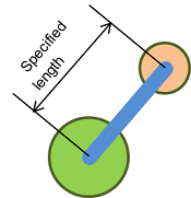
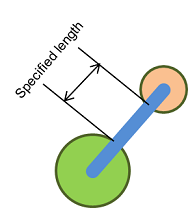
| Length | Specify the value for "Specified length" shown in the diagrams for the Calculation of length field (Real number equal to or greater than 0). | |
| Execute | Attempts to generate fan-outs for the component, or component
pins that you select on the canvas. The Fan-out
Report dialog is displayed. The report contains the
following information.
Component name: the name of the target component. Attempted: the number of target component pins in the component. Routed: the number of component pins that successfully fanned out. Failed: the number of component pins that failed to fan out. |
|
| Exit | Closes the Fan-out dialog without generating fan-outs. |