

In the following table, the items shown in the Item
column can be specified in the Track/Component
tab in the DRC Settings dialog. This dialog
is displayed by clicking Report > Design
Rule Checking > DRC split button >
 DRC Settings
on the ribbon.
DRC Settings
on the ribbon.
- Select Check by an item to include it in the DRC check.
- Select View by an item to show the associated DRC errors on the canvas.
For each check item, the following values are displayed in the table:
- The name of the associated error mark in the Check Results dialog.
- The error mark string that is displayed on the canvas when you execute the DRC command.
Clearance
| Item | Description | Check item | Error mark name in the Check Results dialog | Error mark string displayed on the canvas | |
|---|---|---|---|---|---|
| Clearance | If the specified clearance for the routing pattern is not maintained, then this is identified. The same net is not checked. | Others (distance > 0) | Clearance (clearance) | DRC[layer : gap] | |
| Others (distance = 0) | Clearance (short) | DRC[layer : short] | |||
| For keepout area and layout area | Clearance (inhibit) | DRC[layer : inhibit] | |||
| For hole | Clearance (hole) | DRC[layer : hole] | |||
| Pin of the same net | Clearance (pin) | DRC[layer : pin] | |||
| For negative figure | Clearance (open) | DRC[layer : open] | |||
| In component | If the clearance is not maintained inside data in the same component type, then this is identified. The same net is not checked. See Clearance below. | Distance > 0 | In component clearance (clearance) | DRC[layer : gap-c] | |
| Distance = 0 | In component clearance (short) | DRC[layer : innercomp] | |||
| Via hole | If the clearance between via holes is not maintained, then this is identified. The clearance value is set in the Via hole sub tab, in the Conductor clearance tab in the Rule Editor dialog. The same net is not checked. | Distance > 0 | Via hole clearance (clearance) | DRC[layer : gap-v] | |
| Distance = 0 | Via hole clearance (short) | DRC[layer : viahole] |
Same net
| Item | Description | Check item | Error mark name in the Check Results dialog | Error mark string displayed on the canvas | |
|---|---|---|---|---|---|
| Clearance | If selected, and the clearance of routing patterns in the same
net is not maintained, then this is identified. This clearance
value is specified in the Same
net box, in the Rule Editor
dialog, Conductor
Clearance: Conductor Tab.
Note If In Component is selected in this dialog, then the same net is not checked. |
Distance > 0 | Same net clearance (clearance) | DRC[layer : gap-s] | |
| Distance = 0 | Same net clearance (short) | DRC[layer : short-s] | |||
| Padstack in same net objects | If a via padstack is connected by an area fill, on the conductor
layer, to a component pin or a partially overlapped via padstack,
then clearances can be checked between the via padstack and these
items.
|
- | Same net clearance (short) | DRC[layer : short-s] | |
| Overlapping via | Via shapes are identified that are in the same net, and which overlap each other. | - | Overlapping via | DRC[layer : short-via] | |
| Stacked vias also checked |
|
- | |||
|
Do not detect vias as error that have the same hole diameter |
|
- | |||
| Overlapping track | Track shapes in the same net are identified that touch, but are not considered joined. Area fills in the same net are also detected. | - | Overlapping track | DRC[layer : same-pattern] |
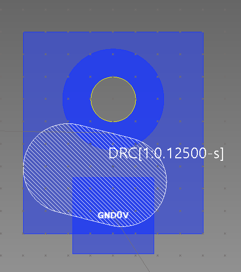
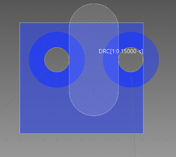
Clearance errors are not detected between pins in the same net.
Restricted connectivity
| Item | Description | Check item | Error mark name in the Check Results dialog | Error mark string displayed on the canvas | |
|---|---|---|---|---|---|
| Overlapping area fill |
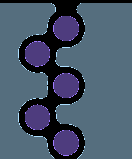
Parts of area fills are identified that are separated from each other by pad clearances in the area fill. Mesh planes are not checked. The following image illustrates how the pad clearances, shown in black, have separated the two parts of the area fill.
|
- | Divided area fill (divided-areafill-compterm) | DRC[layer : divided-areafill-compterm] | |
| - | Divided area fill (divided-areafill-other) | DRC[layer : divided-areafill-other] | |||
| - | Divided area fill (divided-areafill-cutout) | DRC[layer : divided-areafill-cutout] | |||
| - | Divided area fill (divided-areafill) | DRC[layer : divided-areafill] | |||
| Isolated thermal | Thermals are identified that are not connected to an area fill. | - | Isolated thermal | DRC[layer:noconnect] | |
| Malformed thermal | If another figure (thermal land, clearance land, area fill or powerplane) intersects inside the bridge of a thermal, then this is identified. If the inside section is included, then the value for Minimum number of thermal spokes in the Rule Editor Dialog: Tracks Tab is referred to. | - | Malformed thermal | DRC[layer : break-thermal] | |
| Isolated object | For overlapping copper areas, instances are detected whose overlapping width is less than the specified value. This ensures that there is sufficient contact between the relevant copper areas. You can set values specifically for teardrops. This allows you to check teardrops that you add to an otherwise completed design. This section also allows you to detect misaligned tracks, and subnets that have unconnected tracks. | - | Isolated object | DRC[layer : noconnect] | |
| Overlapping width for teardrop | For teardrops on the same net, specify the width of overlaps (real number equal to, or greater than 0). | ||||
| Overlapping width for others | Specify the width of overlaps between a teardrop and a copper object on the same net (real number equal to, or greater than 0). | ||||
| Detect line not on the center | If a track and padstack touch, then this setting allows you
to detect whether the track is connected to the center of the
relevant pad or via.
|
||||
| Detect subnet with unconnected track | This setting allows you to detect subnets that have unconnected
tracks.
|
||||
| Clearance - hole | For clearance lands, if the distance from a hole to a land is smaller than the specified clearance, then this is identified. The clearance configured for a rule area is not referred to. | - | Clearance - hole | DRC[layer : clearance-hole] |
Board Specification
| Item | Description | Check item | Error mark name in the Check Results dialog | Error mark string displayed on the canvas | |
|---|---|---|---|---|---|
| Via layer pairs | This section allows you to set whether an error is displayed if a specified conditional padstack is not used for a particular via layer pair. It also allows you to specify whether an error is displayed if an "available" padstack is used for a particular via layer pair, regardless of whether the specified conditional padstack is used. | Buried via limit violation | Via layer pairs (from-to) | DRC[from-to] | |
| Qualified padstack violation | Via layer pairs (qualifiedPadstack) | DRC[qualifiedPadstack] | |||
| Detect via that violates conditional padstack as error | Allows you to specify whether an error is displayed if a specified conditional padstack is not used for a particular via layer pair. Conditional padstacks are specified in the Rule Editor dialog, Vias tab, Conditional padstack section. If Do not detect available padstack as error is selected, and an "available" padstack is used for a particular via layer pair, then an error is not displayed. Available padstacks are specified in the Rule Editor dialog, Vias tab, Available padstacks section. | ||||
|
Do not detect available padstack as error |
If selected, then an error is not displayed if an "available" padstack is used for a particular via layer pair, regardless of whether the specified conditional padstack is used. Available padstacks are specified in the Rule Editor dialog, Vias tab, Available padstacks section. | ||||
| Invalid buildup vias | If selected, and Use Core Layer
is selected in the Rule
Editor dialog, then the following items are identified by
the DRC command:
If Use Core Layer is not selected in the Rule Editor dialog, then the above items are not identified. Note
|
- | Invalid buildup vias | DRC[buildupvia-layer] | |
| Divided via | Buried vias are identified that overlap vertically at the same position in the same net. | - | - | DRC[min-land-overlap-length] |
Vias
| Item | Description | Check item | Error mark name in the Check Results dialog | Error mark string displayed on the canvas | |
|---|---|---|---|---|---|
| Antenna vias | Vias are identified whose From or To layer is not connected to a track. This DRC check is particularly useful if multiple via spans are specified in the design. It is only available in a High-Speed environment. | - | Antenna vias | DRC[antenna-via] | |
| Divided via | Buried vias are identified that overlap vertically at the same position in the same net. | - | - | DRC[min-land-overlap-length] |
Others
| Item | Description | Check item | Error mark name in the Check Results dialog | Error mark string displayed on the canvas | |
|---|---|---|---|---|---|
| Resist | If a soldering method is defined in the Technology
Editor dialog, for the top and bottom conductor layers, then
resist shapes are identified where the clearance between a resist
shape and a conductor shape is less than the specified minimum
clearance. The recommended procedure for checking this value is
described below.
|
Distance > 0 | Resist (clearance) | DRC[layer : gap-r] | |
| Distance = 0 | Resist (short) | DRC[layer : resist] | |||
| Teardrop | The Teardrops section allows you to identify whether teardrops are generated, and whether they violate the length ratio and track width ratio that you specify. The maximum length ratio is specified in the Design Settings dialog, Teardrops section, Maximum length ratio box. The track width ratio is specified in the Teardrops section, Minimum line width ratio box. | - | - | DRC[layer : teardrop] | |
| Surface mount pin | If selected, then surface mount pads are checked. If no teardrops are generated, or they violate the length ratio and track width ratio, then this is identified. | ||||
| Through hole pin | If selected, then through hole pads are checked. If no teardrops are generated, or if they violate the length ratio and track width ratio, then this is identified. | ||||
| Via/Pad | If selected, then via padstacks that are routed are checked. If no teardrops are generated, or they violate the length ratio and track width ratio, then this is identified. | ||||
| Minimum | Allows you to specify that teardrops are checked that have a line width greater than or equal to the value specified in the associated Line width box. The Line width box is made available. | ||||
| Line width | Allows you to specify the lower line width limit for teardrops. Teardrops are checked that have a line width greater than or equal to this value. This box is made available when Lower limit is selected. | ||||
| Maximum | Allows you to specify that teardrops are checked that have a line width less than or equal to the value specified in the associated Line width box. The Line width box is made available. | ||||
| Line width | Allows you to specify the upper line width limit for teardrops. Teardrops are checked that have a line width less than or equal to this value. This box is made available when Upper limit is selected. | ||||
| Track width | Tracks are detected that violate the maximum track width and
minimum track width that is set using the track width stacks specified
in the Rule Editor
dialog. Track width stacks are created for E-nets and nets
in the Rule Editor
dialog, Tracks tab. They are created for differential pairs
in the Rule
Editor Dialog: Differential Pairs Tab. The track width stacks
that you create can be applied to tracks as follows.
|
Maximum track width violation | Track width (maximum width) | DRC[layer : maxlinewidth] | |
| Minimum track width violation | Track width (minimum width) | DRC[layer : minlinewidth] | |||
| Land status | Differences are identified between the land status that is set in the Change Land Status dialog, and the actual status of the land. For example, a land status of Unconnected would be identified as an error for a connected pad. | Land status | Land status | DRC[layer : Current->Normalization] Example) DRC[1 : CON->UNC] |
|
| Connected | Land shape (connect) | DRC[layer : landshape-connect] | |||
This error is shown if a padstack is specified that has a bigger
drill size than the pads. This can result in a short between planes,
because there is no clearance between mechanical holes and area
fills. It can be prevented by avoiding padstacks which have a
bigger drill than the pads. The following solutions are also recommended.
|
Unconnected | Land shape (noconnect) | DRC[layer : landshape-noconnect] | ||
| Thermal land | Land shape (thermal) | DRC[layer : landshape-thermal] | |||
| Clearance land | Land shape (clearance) | DRC[layer : landshape-clearance] | |||
| Antenna track |
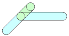
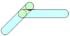
If selected, routing patterns are identified that are considered antennas. Antennas are identified according to the position of the circular end point of a line. In the following example, an antenna track is identified as the circular end point of the first line does not overlap the second line.
In the following example, an antenna track is not identified as the circular end point of the first line overlaps the second line.
|
- | Antenna track | DRC[antenna-wiring] |
Component
| Item | Description | Check item | Error mark name in the Check Results dialog | Error mark string displayed on the canvas | |
|---|---|---|---|---|---|
| Component clearance | If the specified clearance between component areas is violated, then this is identified. This setting is specified in the Component area - Component area box, in the Rule Editor dialog, Placement tab. | Component clearance | Component clearance | CMPDRC[ Cmp ] | |
| Placement keepout area | Component clearance (Placement keepout area) | CMPDRC[ PInh ] | |||
| Height limit area | Component clearance (Height limit area) | CMPDRC[ Hei ] | |||
| Layout area | Component clearance (Layout area) | CMPDRC[ Lay ] | |||
| Component position | Components are identified that violate the specified settings for placement side or placement angle. These settings are specified for a component in the Permitted Placement Side and Permitted Placement Angle columns, respectively, in Constraint Browser. | Angle (Rule, CDB) | Component position (Angle) | CMPDRC[ Ang( Rul CDB )] | |
| Placement side (Rule, CDB, soldering, package, conductor area) | Component position (Side) | CMPDRC[ Side( CmpRul CDB Sol Pkg LayRul )] | |||
| Component group included | Group area | CMPDRC[ InGrp ] | |||
| Check for component group | If selected, and a component group exists in the design, then an error is displayed if it does not contain all associated components. | ||||
| Component placement (manhattan length) | In a High Speed environment, this settings allows you to check
the manhattan length of a pin pair.
Note In Constraint Browser, the actual routed length of the pin pair is checked, rather than the manhattan length. This value is shown in the Actual column, in the High Speed Routing Tab, Pin Pair Length section. |
||||
| Component placement (manhattan length) | Component placement (manhattan length) | CMPDRC[ NetMax ] | |||
| Pin pair maximum track length (manhattan) (Net) | Component placement (pin pair net manhattan length) | CMPDRC[ NetPPMax ] | |||
| Pin pair maximum track length (manhattan) | Component placement (pin pair manhattan length) | CMPDRC[ PPMax ] |
